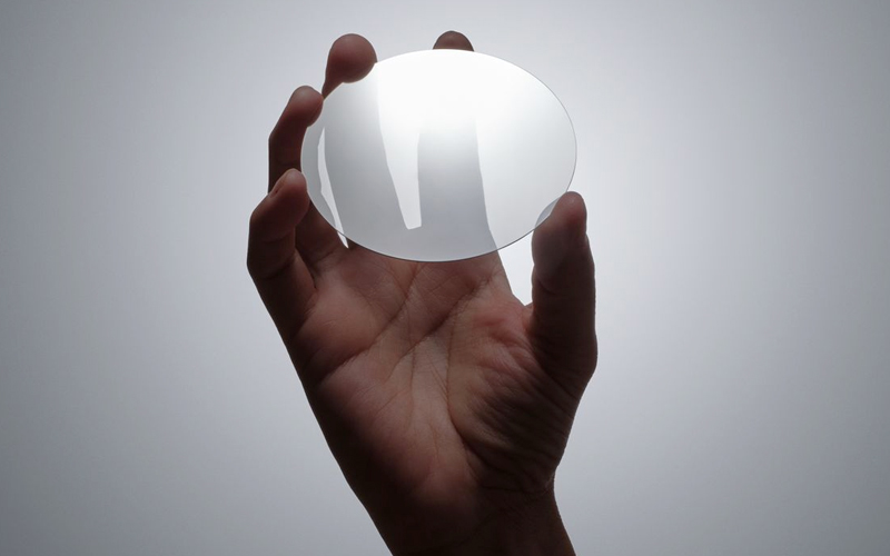
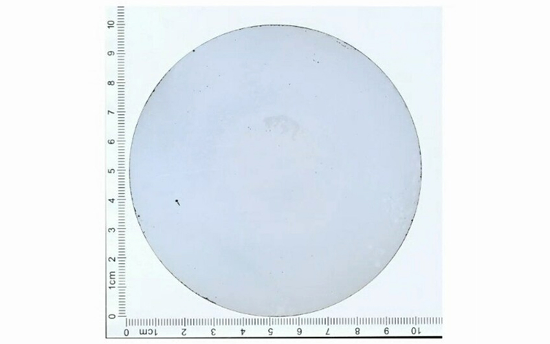
In November, 2023, Diamond Foundry (DF) produced the world’s first 100mm single-crystal diamond wafer. However their end-game has nothing to do with high carat weight – and everything to do with high thermal loads.
Lab Grown Diamonds x Computers
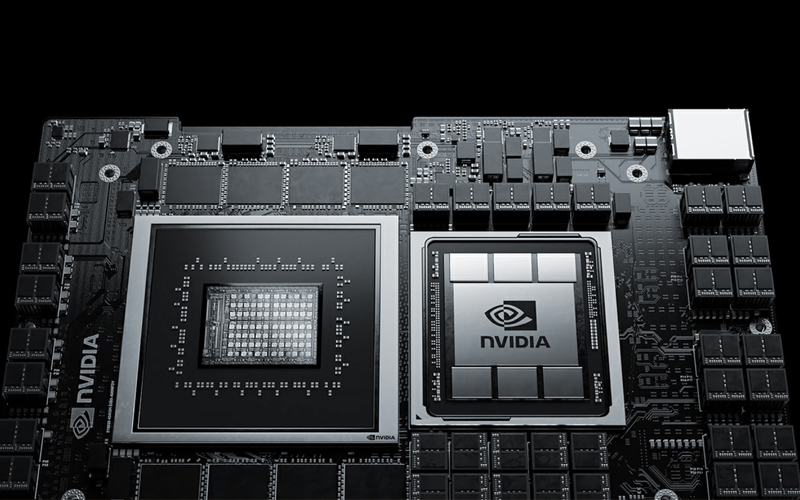
Microchips get hot. The more processing that is required, the hotter they get. That limits the amount of electricity which can be pushed through a chip. In fact heat is the #1 limiter of how fast a microchip can run. For over a half-century this has been a primary design consideration in the building of supercomputers and, more recently, new applications involving artificial intelligence.
That brings us to diamonds, which can carry high thermal loads better than any other substance known to humanity… And to Diamond Foundry, which is using a technology called heteroepitaxy to create these single-crystal diamonds on scalable substrates. According to the Wall Street Journal, the company has run tests on an unspecified high-end Nvidia GPU which uses synthetic diamond wafers, and claims to have clocked three times the recorded performance versus standard manufacturing materials.
Lab Grown Diamonds x Cars
Around the same time DF was touting their 100mm achievement, the Washington State based producer announced that it had created an electric car inverter, leveraging diamond wafer technology to enable more efficient electric cars. Not only is their power electronics unit six times smaller than that of a Tesla 3, they claim it also delivers more power more efficiently.
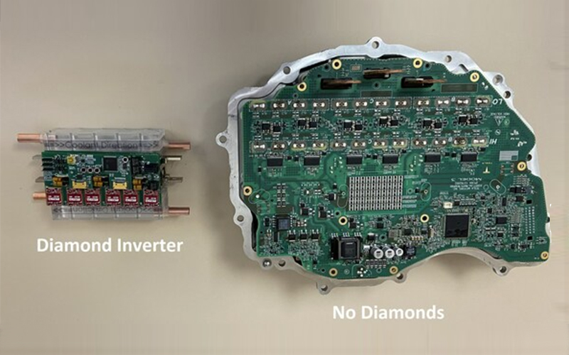
According to Diamond Foundry: “The design of power semiconductors is essentially driven by two factors: Thermal conductivity – the path to cool them down – and electrical conductivity – the path to carry high currents. Though the electrical path has been worked on for many years with more or less success, the thermal path has always been the main challenge. Further, power semiconductors need to be isolated from the rest of the environment because of safety required with high voltages. Voltage isolation barriers usually demonstrate poor thermal conductivity.”
“Diamond wafers can now be employed using two of its extreme properties: extreme thermal performance plus extreme electrical insulation. The advent of cost efficient diamond wafers creates fundamental new design opportunities for power electronics in ways not possible before. With the benefit of these new designs being so stark, it is hard to see them not to become the standard in power electronics.”
DF’s next goal is to further reduce the defect density of its diamond wafer to achieve the textbook semiconductor “figure of merit” for diamond, which is 17,200 superior to silicon and 60 times superior to silicon carbide.
We’ll be watching…

and is the culmination of a project that began 30 years ago, according to the company.